Push-Pull driver PCB
NEW 2/10/13 - Posted details of the "807" Push-Pull amp using this board (on its own page)
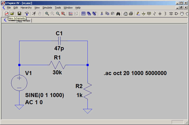
I've been working on another PCB - this one is a mono push-pull driver board.
The idea was to make something a little like the "red board", but more flexible. You can use any output tube or power supply, because they are not on the PCB. You can build stereo or mono (the board is only one channel). You can use a first stage and apply NFB (or not), or you can jumper around the first stage and make a 2 stage amp. You can use local feedback to the driver plates from the output plates or ultralinear taps, or not.
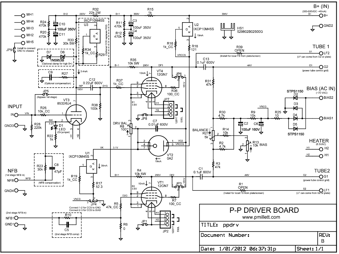
Here's the schematic, as of 12/27/11, showing values I'm using for a KT88 triode amp (or download a PDF file):
Circuit Description
First stage
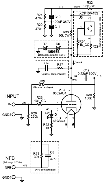 The
first stage uses a single triode, 8532 or 6J4 (VT1). If a 2-stage
amplifier is built and the first stage is not needed, all of the components
shown here are omitted, and a small wire jumper is installed at JP5 (located
underneath R28, which would not be installed).
The
first stage uses a single triode, 8532 or 6J4 (VT1). If a 2-stage
amplifier is built and the first stage is not needed, all of the components
shown here are omitted, and a small wire jumper is installed at JP5 (located
underneath R28, which would not be installed).
Working from the input pads ("IN" on the PCB, and a ground pad) R28 is a grid leak resistor, providing the path to ground from the grid. 100k - 470k is typical. R26 is a grid stopper to prevent spurious oscillation; 1k - 10k carbon composition resistor would typically be used.
On the cathode of the input tube, R22 provides cathode bias. It is un-bypassed, as this node is typically used to inject negative feedback. In series with R22 is an optional 3mm LED. If not using NFB, you can use the LED to bias the input tube. If not using the LED, install a wire jumper in its place. Or you can use both in series... the LED will provide a constant voltage, and the resistor will still allow the injection of NFB to the cathode.
Global negative feedback can be applied to the first stage at the NFB pad. A ground pad is located adjacent to the NFB pad. Typically a twisted pair of wires would connect from here to the OPT secondary, or to the output jacks.
The value of R23 and R22 set the amount of negative feedback - R23 and R22 are a voltage divider. The smaller R23 is, the more NFB is provided.
To provide lead compensation to make the amplifier stable with global NFB, a capacitor C8 is placed in parallel with R23. The value of this cap can be estimated by making open-loop measurements of the amplifier phase shift at high frequency. This cap (along with R22 and R23) provides a pole and a zero in the feedback path, which gives you a phase lead. This phase "bump" will counter the phase lag of the amplifier (largely caused by the output transformer).
On the plate, C12 is a coupling capacitor on to the second stage. Usually 0.1 to 0.47uF, 600V. With NFB, you may need to tweak the value up or down to avoid low frequency peaking, depending on your OPT.
C9 and R27 provide an optional "step" network at high frequencies. This provides some rolloff at high frequency; again, a pole and a zero. Normally this network is not needed, but if stability cannot be achieved using the lead compensation alone, sometimes this will help. Note that the value of the plate load resistor in parallel with the Rp of the tube will affect the frequency response as well.
D6 and D7, two zener diodes in series, can be used to provide a clamp on the plate voltage of the input tube. The 8532 has a maximum plate voltage rating of 150V, which means that the absolute highest voltage that is expected to appear is less than twice that, or 300V. If using high B+ (say, 600V), if B+ rises while the tube is cold, it could arc or damage the input tube. These zeners will clamp the voltage.
R33 is the plate load resistor. It, along with R22, will affect the gain of the first stage, as well as have an impact on distortion. Optionally, R33 can be replaced with a constant current source load, composed of U3, R29, and R34. R34 is to help prevent oscillation (a 1k carbon comp is advised), and R29 sets the current.
Finally, R32 and C10/C11 provide power supply decoupling (and also a drop of voltage if desired). Two electrolytic caps are provided in series, with equalizing/ bleeder resistors R20 and R24, in case high B+ voltages (over 450V) are desired.
Second stage
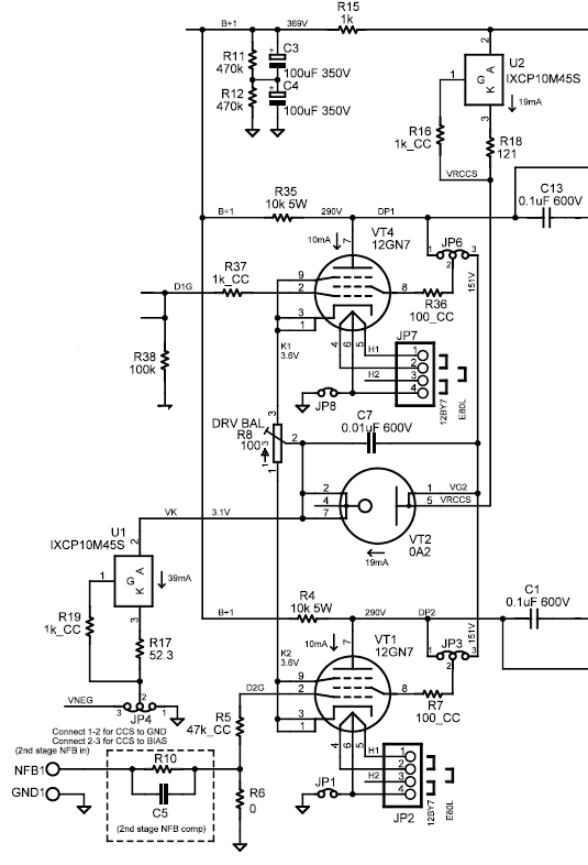 The
second stage is a differential amplifier using pentodes. The PCB can accommodate
many different 9-pin pentodes, which fall into 2 basic pinout groups: One
is the 12BY7, which also includes similar tubes like the 12HG7, 12GN7, 12HL7,
and 11HM7. The other is the E80L, which allows a great number of tubes,
including the EF184/6EJ7 and other high gm pentodes.
The
second stage is a differential amplifier using pentodes. The PCB can accommodate
many different 9-pin pentodes, which fall into 2 basic pinout groups: One
is the 12BY7, which also includes similar tubes like the 12HG7, 12GN7, 12HL7,
and 11HM7. The other is the E80L, which allows a great number of tubes,
including the EF184/6EJ7 and other high gm pentodes.
Jumper blocks JP7 and JP2 allow configuration for the 12V center-tapped-heater tubes (12BY7-types) or 6V types. You can install wire jumpers, or a 0.100" header and use shunts to select which is connected. In addition, a small wire jumper is provided on pin 6 of the tubes (JP8 and JP1) that provides a short connection from pin 6 to ground, for tubes that use pin 6 as an internal shield.
The input to the grid of the upper tube, VT4, is provided with a grid stopper resistor R37 (again, typically a carbon comp resistor) and a grid leak resistor R38. Check the tube datasheet to see what the largest value of grid leak resistor is allowed.
The grid of the lower tube, VT1, has a similar grid stopper (R5) and grid leak (R6) resistor. Two resistors are used here to allow the connection of NFB to this input of the differential amp, if desired. This could be done if building a 2-stage amp, or even if the first stage is used without feedback. As in the first stage, R10 (along with R6) form a voltage divider that sets the amount of NFB, and C5 can be installed to provide lead compensation.
If not using NFB here, you need to be careful about the value of R5 and/or R6. If using a negative voltage on the CCS (see below), the grid, which sits at 0V, will become a virtual plate if B+ has not yet been applied. So the grid will try and conduct all the current that the CCS can supply. I used a large grid stopper (47k) to limit this current. Note that as soon as B+ is up, the plate will take all the current and the grid will be safe.
In the cathode circuit, a pot (R8) is used to allow adjustment of the balance of the stage. The wiper of the balance pot is connected to a CCS circuit, comprised of U1, R19, and R17. R19 is a stopper (carbon comp) and R17 sets the current. Note that the current in this CCS is the sum of the cathode currents of the two tubes, and well as the current through the VR tube VT2.
A wire jumper JP4 allows connection of the CCS to ground (jumper pins 1 & 2), or to the negative voltage supplied by the bias supply (jumper pins 2 & 3). Note that the compliance range of the CCS limits operation connected to ground to a cathode bias voltage of above 4-5 volts; below that the CCS will stop acting like a CCS and distortion will shoot up.
The screen grids are provided with grid stoppers (R36 and R7), typically carbon comp. The screens can be jumpered to the plates to triode-connect the tubes if desired, by installing wire jumpers between pins 1 & 2 of JP6 and JP3. If pentode operation is desired, install wire jumpers between pins 2 & 3.
In pentode mode, screen voltage is provided by a CCS circuit (U2, R16, and R18) and is regulated by a VR tube VT2. The CCS current (set by R18) is set to around 20mA. Again, R16 is a stopper (carbon comp). The cathode of the VR tube is connected to the tail CCS, so when setting the tail current, keep in mind that this additional 20mA is also passing through that CCS.
If operating in triode mode, you can omit the VR tube and CCS (VT2, U2, R16, and R18).
The plates of the tubes are connected to resistive loads, R35 and R4. The voltage to these loads is decoupled by R15 and C3/C4, again two series-connected electrolytics with equalizing / bleeder resistors R11 and R12.
The output is taken from the plates by coupling capacitors C13 and C1, again, typically 0.1uF to 0.47uF, 600V.
Another connection from the plate to a pair of resistors is provided to implement plate-to-plate local feedback ("Schade" feedback), or connection to ultralinear taps on an OPT ("E-linear" connection).
Bias and output section
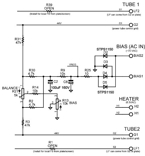 As
mentioned above, resistors R39 and R1 can be installed to provide local feedback
to the driver plates. This would typically be connected to the output tube
plates ("plate-to-plate" feedback), or to ultralinear taps on the OPT
("E-linear" feedback).
As
mentioned above, resistors R39 and R1 can be installed to provide local feedback
to the driver plates. This would typically be connected to the output tube
plates ("plate-to-plate" feedback), or to ultralinear taps on the OPT
("E-linear" feedback).
Circuitry is provided to generate a DC bias voltage for the power tube grids, as well as to provide a negative voltage to connect the tail CCS of the second stage. From the pads labeled BIAS, a full-wave bridge rectifier consisting of D2 - D5 rectifies an AC input voltage. Schottky or fast-recovery diodes are suggested here, as diode reverse recovery noise can make it's way into the grid circuit if you use normal silicon diodes.
An RC filter (R25 and C6) provide the first stage of filtering to generate a negative DC voltage. This point is tapped and provided as the negative voltage for the tail CCS (above).
A second stage RC filter (R9 and C2) provide additional filtering to generate the negative bias voltage for the output tubes.
The network of resistors and pots R30, R2, R21, R14, and R13 provide the bias adjustment circuit for the output tubes. Though it looks a little strange, the circuit is configured as shown so that if the wiper of a pot ever opens (entirely possible, it's a mechanical thing), the bias defaults to full negative. No reason for a bad pot to fry your output tubes...
The whole network is just a voltage divider (so be aware your rectified bias voltage needs to be a bit more than the voltage needed to bias the tubes). R30 and R2 provide the top part of the dividers, from the bias supply to the balance pot, R21. The wiper of R21 is then connected to a series resistor R14, which sets the most positive that the bias can be (if it were zero ohms, the bias could be adjusted to 0V - usually not a good thing). Adjustment of the bias voltage is then made by the last leg of the divider, the bias pot R13.
Note that you will probably have to make changes to these resistor values to get the bias level that you want on your amplifier.
Finally, R3 and R31 provide grid leak and bias voltage to the output tubes. Again, be careful how big you make these - I've found more than 47k is risky, as some output tubes draw a wee bit of grid current.
Oh, one other thing - the heaters of the tubes are connected to a pair of pads. You will want to connect one side or the center tap to ground, or to an elevated voltage, to prevent noise.
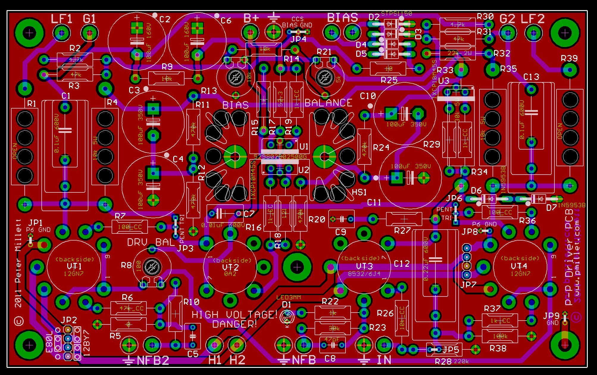
Here's the PCB:

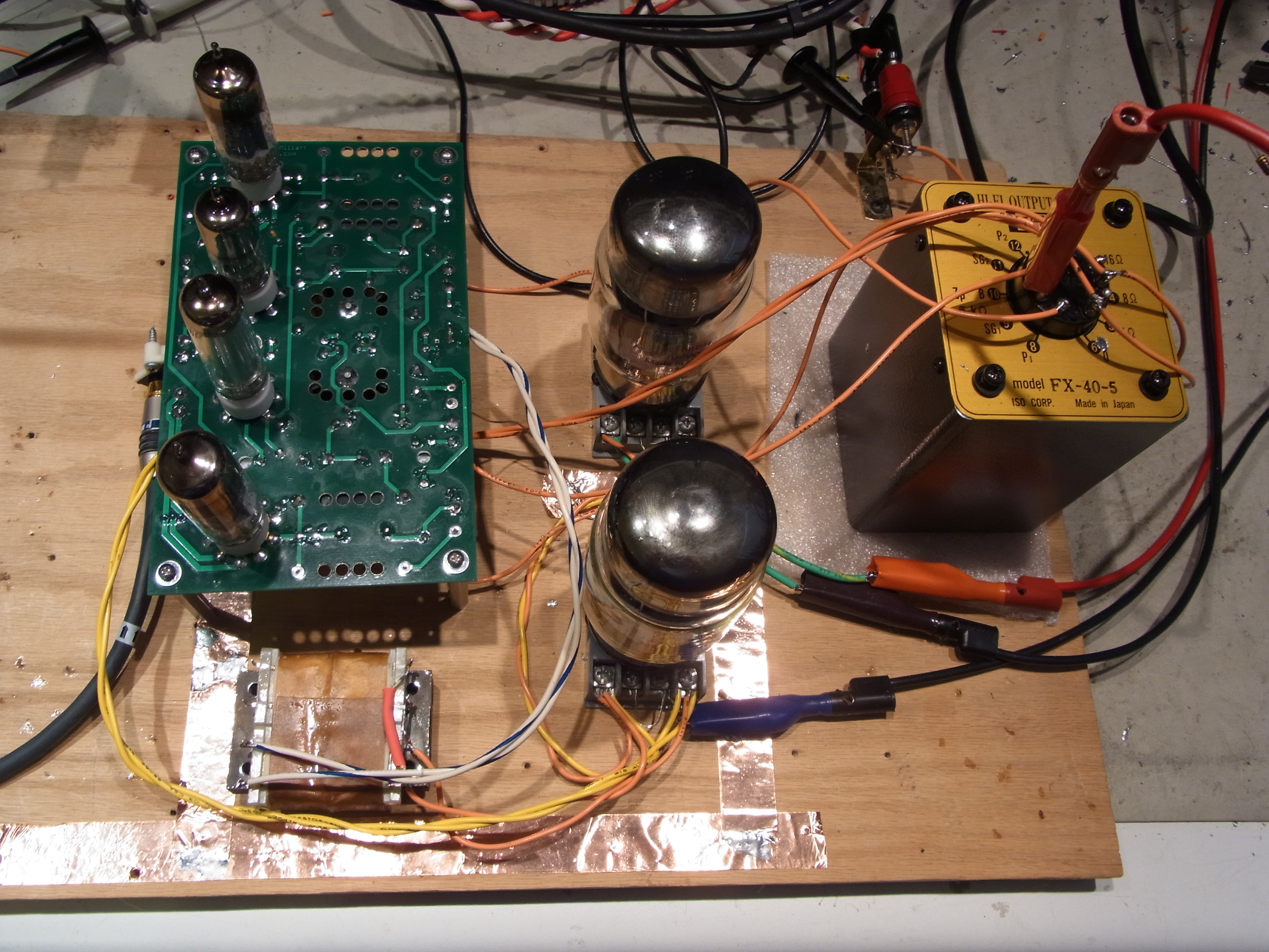
12/24/11 - I now have one of the prototype PCBs stuffed and running. I have it set up as a triode-connected KT88 amp.

The PCB works MUCH better than the breadboard did, in terms of stability. It now acts the way the math says it should. I guess there were too many parasitics (stray capacitance, etc.) on the breadboard.
For comparison, here's the original breadboard:
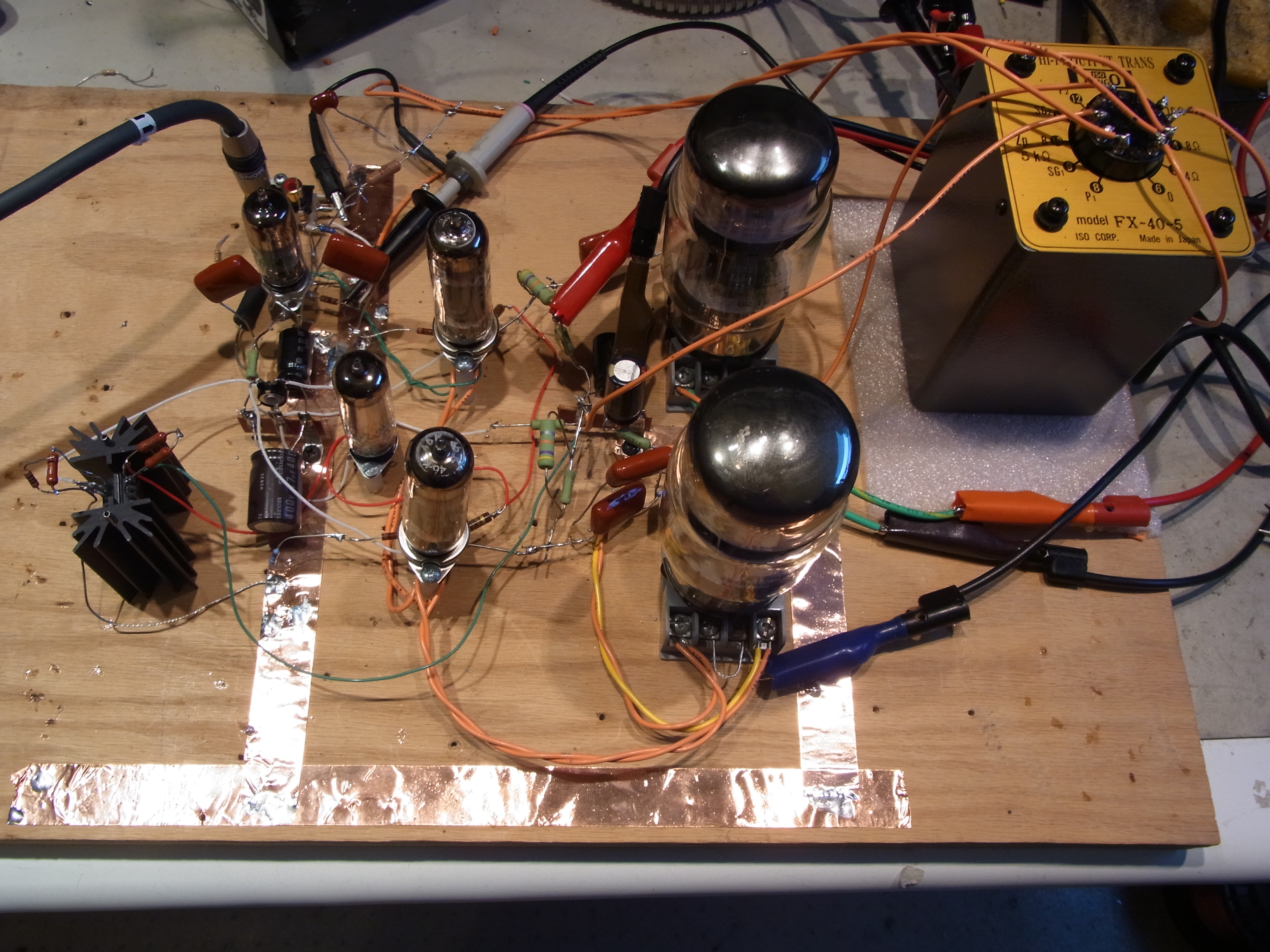
The amp on the breadboard is push-pull triode-mode KT88s, running fixed bias with a plate voltage around 400V, and Tango FX-40-5 output transformers (5k plate-to-plate).
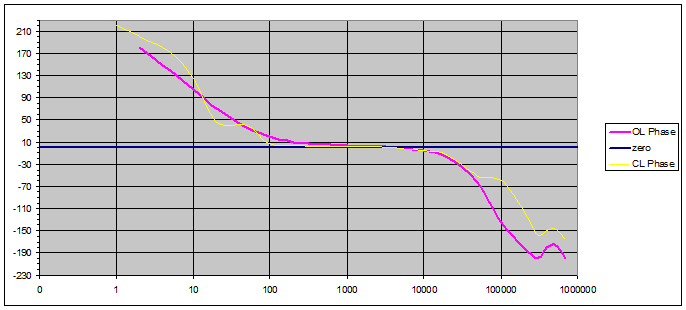
Stability and global NFB
The KT88 triode amp is using global NFB. To figure out the compensation needed to keep it stable, I did open-loop gain and phase measurements (a Bode plot):
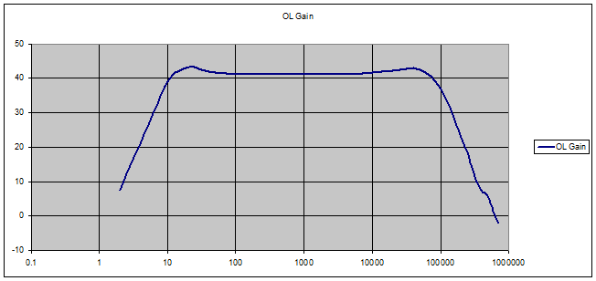
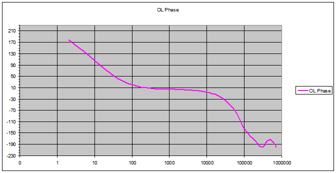
The amp without NFB has a gain of around 40dB. If you look at the phase plot, you can see it crosses 180 degrees at about 200kHz (and again around 400kHz). A good portion of this phase shift comes from the OPT (Tango FX-40-5). At 200kHz, it still has about 23dB of gain.
I wanted the amp to drive to full output (which in this case is around 23 watts) with a 1V RMS input. To do that, I need a closed-loop gain of about 28dB. So, I need around 12dB of negative feedback. If I apply this feedback with no compensation, I will still have 11dB of gain at 200kHz, where the phase crosses 180. What does that mean? That it will oscillate at 200kHz. And yes indeed, it does.
To fix this, you need "lead compensation", an RC network in the feedback path that will cause a phase "bump" in the area where the open-loop phase is approaching 180 degrees.
Rather than try and show you the math, here's a simulation of the network I used (thank you, Linear Tech!):
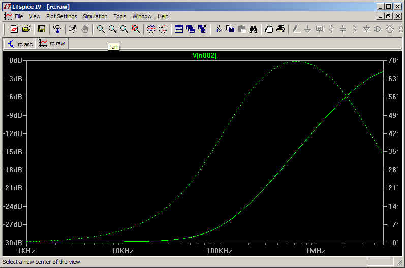
You can see from the plot that you would expect this circuit to give you about a 70 degree phase bump centered around 600kHz.
Running Bode plots with the loop closed, I get this:
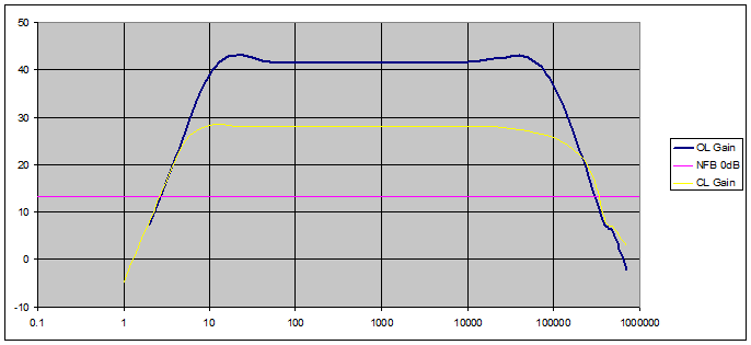
You can see the result of the lead compensation. The amp is stable.
You can download the .XLS file with this data if you are interested.
Now, for measurements of the amp:
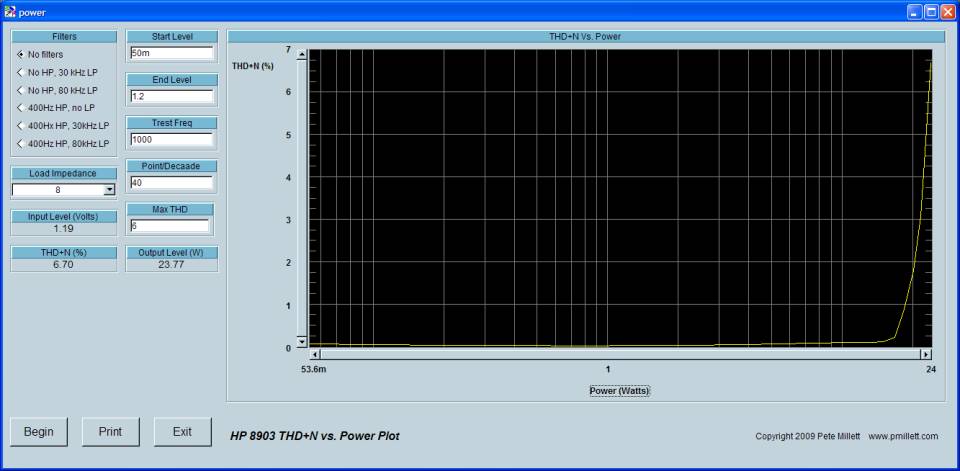
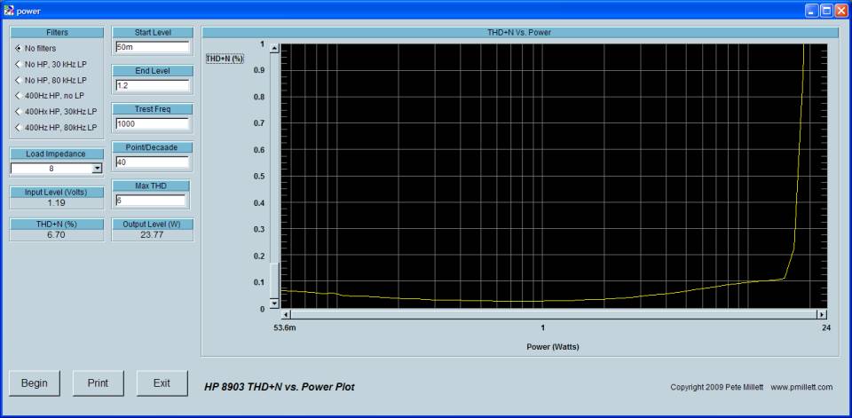
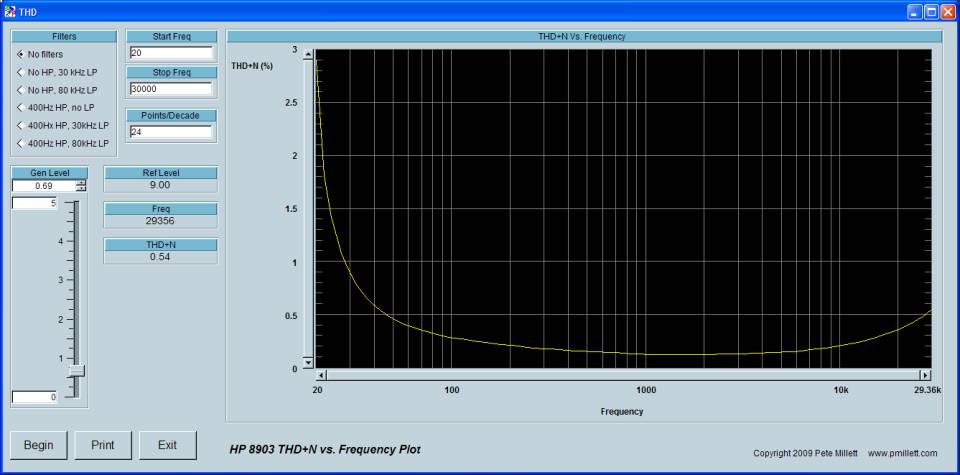
THD+N vs. output power (same plot twice with different Y scales) - just under 24 watts at clipping:
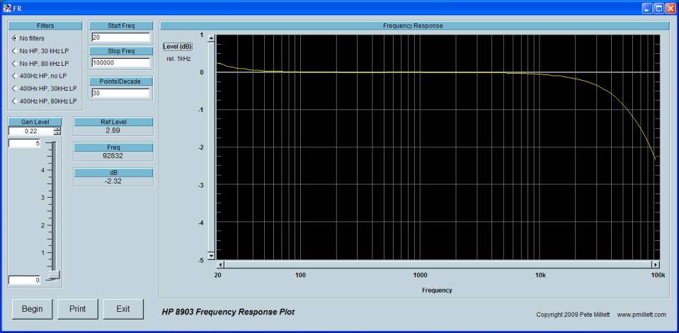
Frequency response @ 1 Watt into 8 ohms - note a small bump at ~15Hz due to the feedback and phase shift in the OPT (it drops back down below 10Hz) :
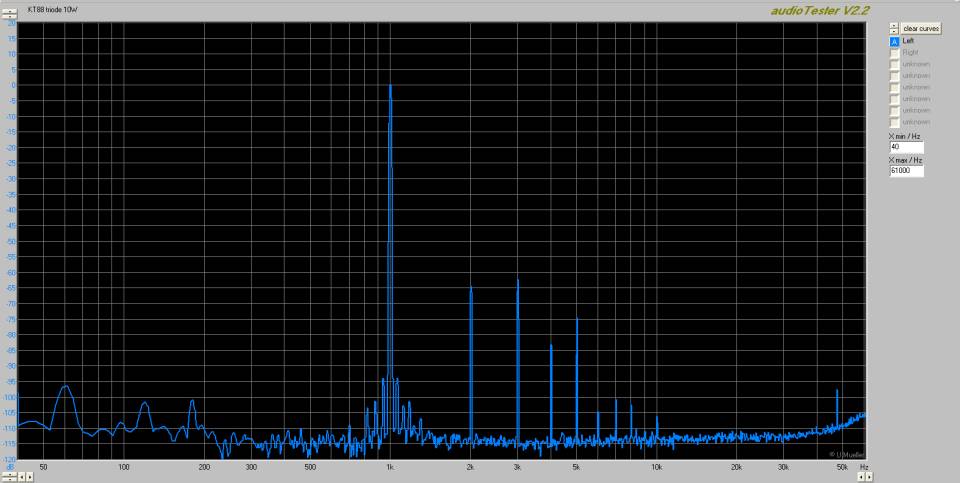
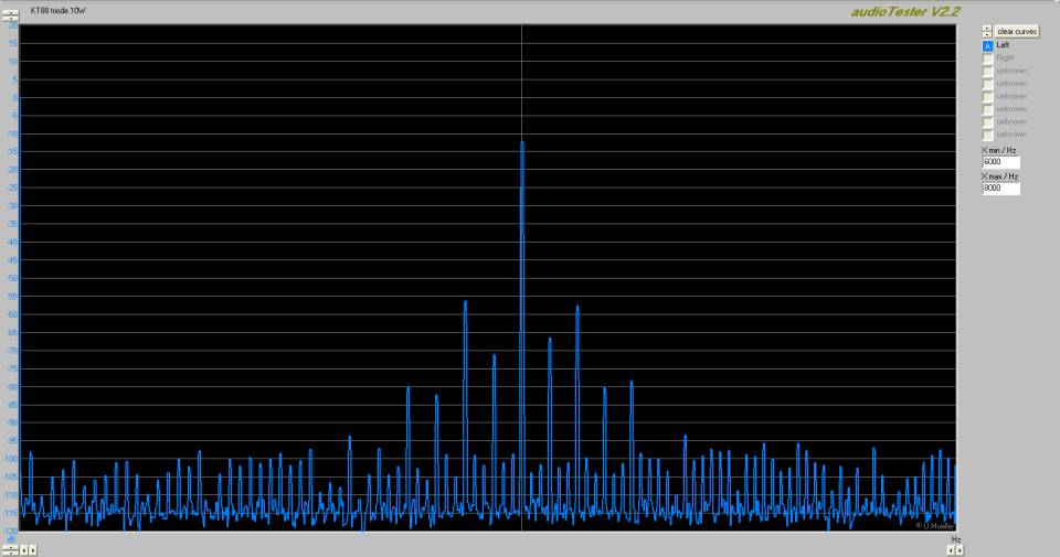
...and at 10 watts:


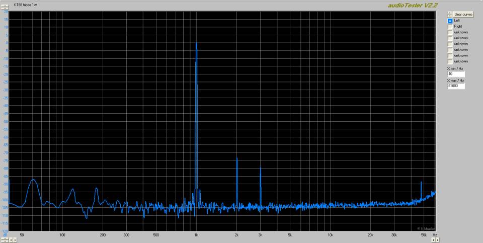
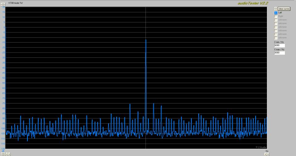
FFT at 1kHz 1W (48kHz tone is a measurement artifact - some test equipment power supply):
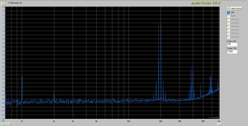
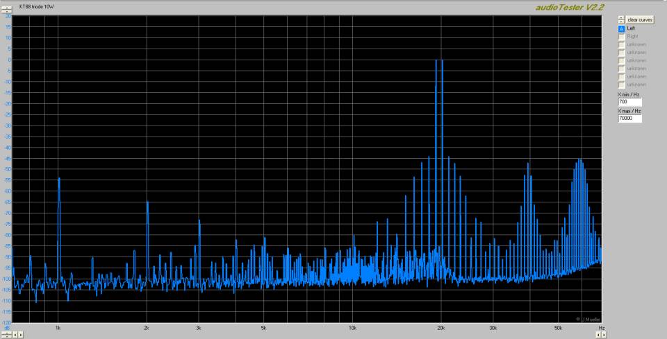
19kHz + 20kHz IMD spectrum @ 10 watts - 1kHz is -55dB or 0.18%:
7kHz + 60Hz 1:4 IMD spectrum @ 1 watt - highest peaks are -63dB from the 7kHz tone:
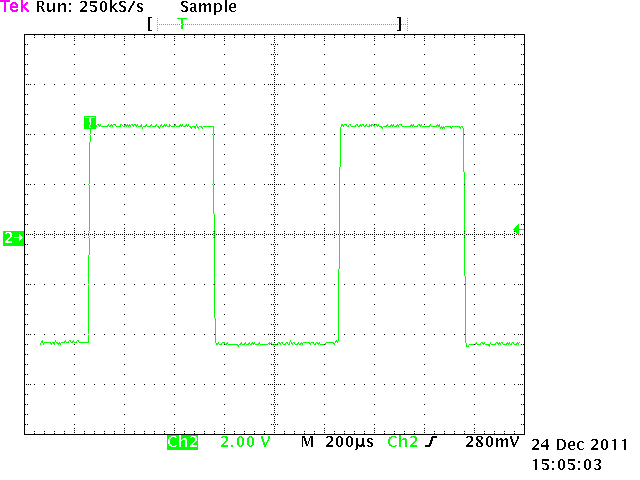
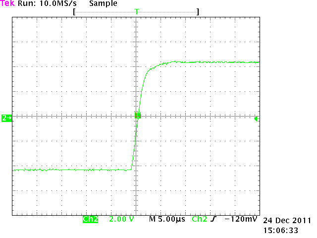
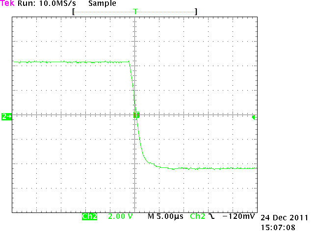
Square wave response (~4V RMS, no significant change with amplitude, or even with no load - good HF stability) (this is a 500MHz scope, so nothing hiding!):
I also made a little board to hold a pair of snapmount caps to along with this project. I got tired of gluing/clamping them to the chassis.
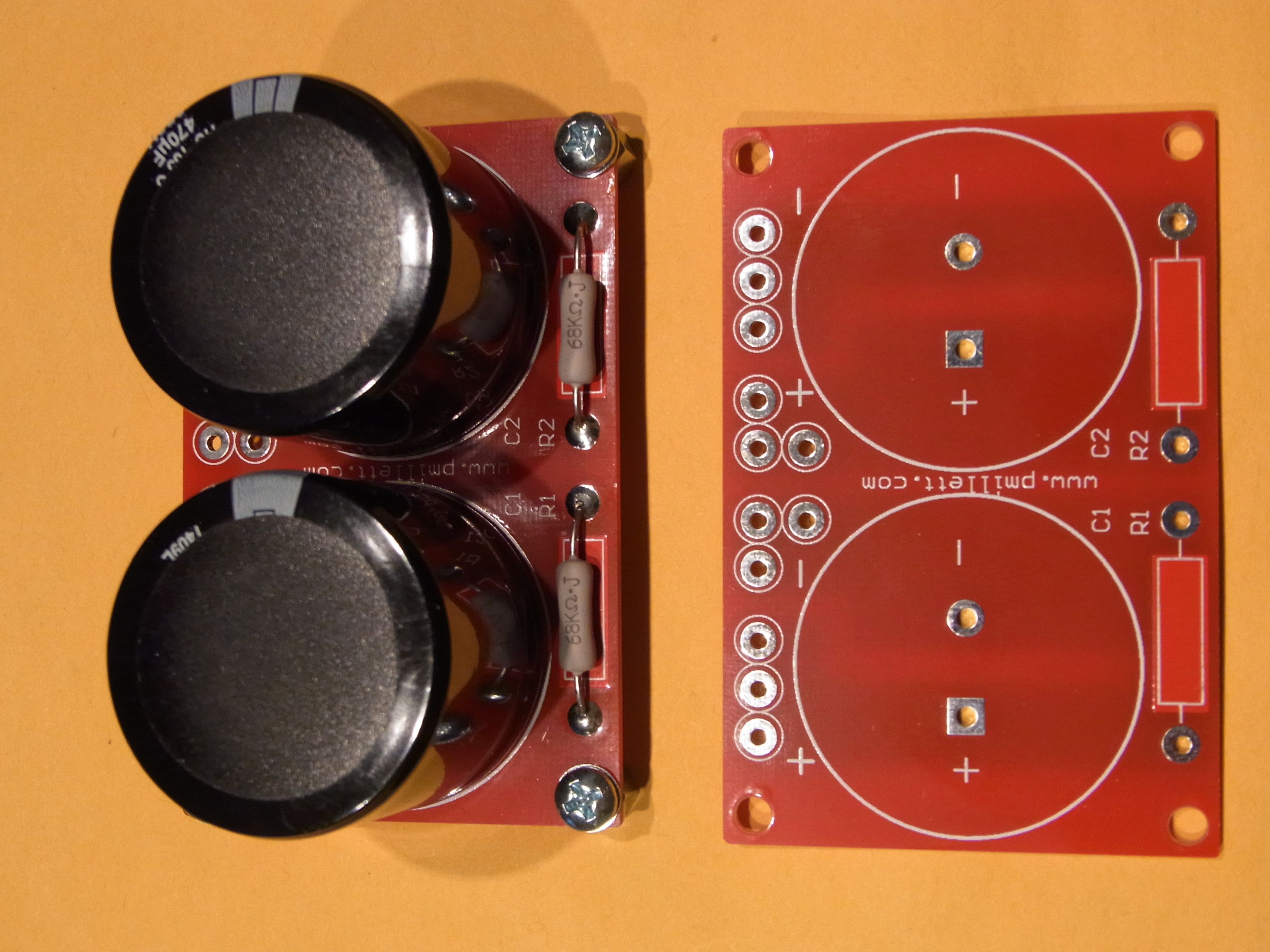
It holds snap mount caps up to 35mm in diameter. It has spots for 2W (or small 5W) bleeder resistors, and is arranged to you can easily connect the two in series for >450V supplies.
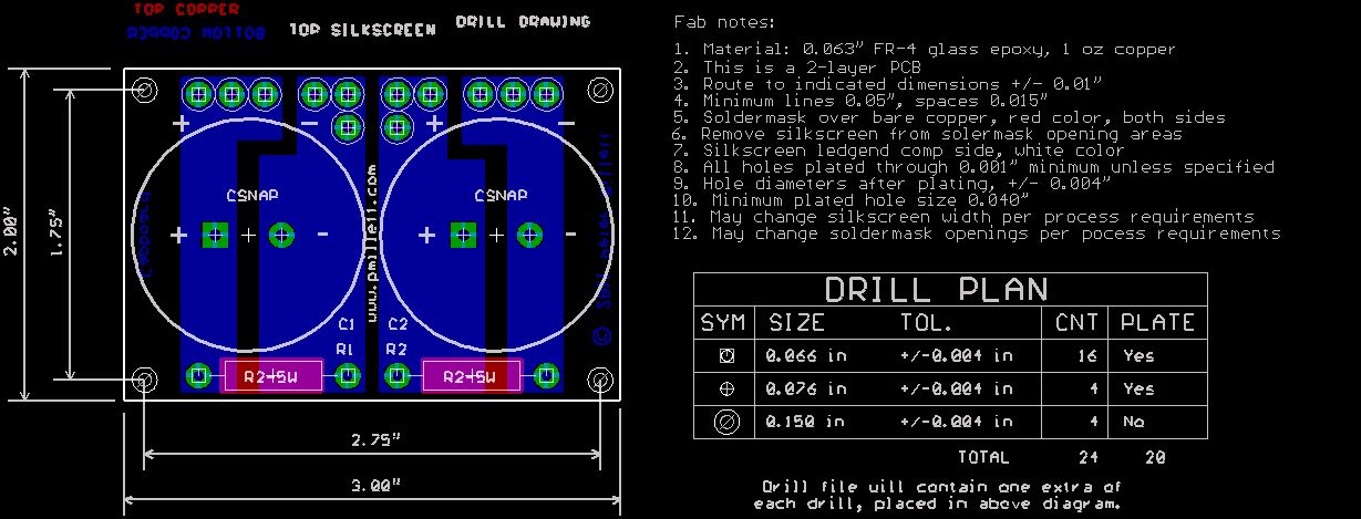
Here is a PDF file with the dimensions. The mounting holes are 0.150" diameter and will accept 3,mm or #6-32 screws.
This PCB is available on eBay.